Blog
Various Semiconductors
Band Structure
When atomic orbitals interact to form molecular orbitals, two energy levels are formed: low-energy bonding orbitals and high-energy antibonding orbitals. In a crystal structure with a large number of atoms, the number of bonding and antibonding orbitals increases because all atoms interact with each other. Since there is an upper limit to the magnitude of the energy splitting and only the number of states is enormous, the possible energy levels of the electrons in the crystal are nearly continuous. This structure is called the band structure. Since electrons are occupied from the more stable lower energy levels, a low-energy band filled with electrons and a high-energy band without electrons appear. Each band is called "Valence band" and "Conduction band". The formation of the band structure is shown in Figure 1.

Figure 1. Formation of band structure
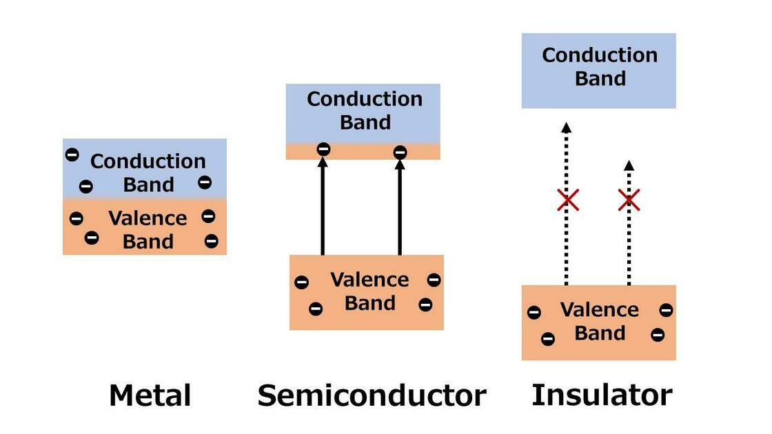
Between the valence band and the conduction band, some materials have an energy region where electrons cannot exist (forbidden band). The width of this forbidden band is called the band gap. When energy is applied to a crystal by voltage or light irradiation, electrons in the valence band are excited and move into the conduction band. Crystals with no band gap are called conductors (metals), and those with a band gap so wide that electrons cannot transition even when energy is applied are called insulators. Their band structure diagrams are shown in Figure 2.
Those with a band gap somewhere between that of an insulator and a conductor are called semiconductors. There is no clear definition of the difference between semiconductors and insulators, and there are also wide-gap semiconductors with very wide band gaps (see below for details).

Figure 2. Band structure of each
Wide-bandgap Semiconductor
The most widespread semiconductor material today is silicon (Si). The band gap of silicon is 1.12 eV, but semiconductors with a band gap larger than this value are called wide-gap semiconductors, such as SiC and GaN. Materials with a wide band gap are characterized by a small lattice constant and strong interatomic bonding. The strong bonding between atoms makes the energy state of electrons very stable, which allows a large band gap to be formed. This characteristic allows semiconductor devices that can be driven in high-temperature environments to be created because the electrons are not excited and retain their semiconductor properties even in high-temperature environments. The breakdown electric field strength is also much higher than that of Si. This makes it possible to apply large voltages and to develop devices with high saturation drift velocity (maximum velocity of charge carriers when voltage is applied) and high speed drive.
Direct Bandgap and Indirect Bandgap
There are two types of electron transitions in semiconductors: direct transitions and indirect transitions.
Direct transitions are those in which the wave numbers at the top of the valence band and the bottom of the conduction band coincide. In semiconductors with direct transitions, the energy of the excited electron is emitted as a photon. Therefore, direct-transition semiconductors have high luminous efficiency and are used in light-emitting diodes and semiconductor lasers.
Indirect transitions are transitions in which the wave numbers at the top of the valence band and the bottom of the conduction band do not coincide. Therefore, excitation and relaxation require the exchange of momentum as well as energy. Momentum exchange is often mediated by lattice vibrations (phonons), i.e., heat, and the luminescence efficiency is extremely low. Figure 3 shows a schematic diagram of direct and indirect transitions in momentum space (k-space).

Figure 3. Direct bandgap and indirect bandgap
Limitations of Moore's Law and Two-Dimensional Semiconductors
In the modern semiconductor device industry, miniaturization and integration are progressing toward lower cost in fabrication, higher operating speeds, and more advanced functionality. In particular, integrated circuits, which form microscopic electronic circuits on the surface of semiconductors, are expected to increase in computing power as the number of transistors on the circuit increases. The miniaturization of integrated circuits has developed in accordance with Moore's law, which states that the number of transistors per integrated circuit doubles every year. However, the limit to making transistors using Si, a three-dimensional semiconductor, any smaller than they are now is being reached. The reason for this is that making Si too small causes the interface to become unstable and physical properties to disappear. Two-dimensional semiconductors are a candidate for a new material that can break through this problem.
Two-dimensional semiconductors have a two-dimensional structure, in which atoms are bound together in sheets, making them very thin and facilitating device miniaturisation. Graphene is a typical two-dimensional semiconductor. This is a two-dimensional material composed entirely of carbon atoms. Graphene has a special band structure, the Dirac cone structure, in which the π and π* orbitals do not overlap each other and the upper end of the valence band and the lower end of the conduction band are in contact only at six points.1 For this reason, graphene is also called a zero gap semiconductor. Therefore, graphene cannot be used as a two-dimensional semiconductor as it is, and defects must be created by doping or ion implantation. Another problem is that the cost of creating it is very high. Transition metal dichalcogenide (TMDC) is attracting attention as a material that solves this problem. The physical properties of TMDC vary, depending on composition and crystal structure, and include metals, semi-metals, semiconductors and insulators. Unlike graphene, TMDCs have semiconducting properties from the outset and can be used directly in devices without the need for processing. Research is being conducted worldwide to develop devices that make use of these characteristics.